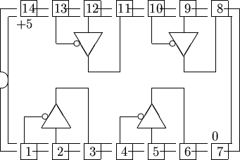
Three-state logic
As a tri-state digital circuit elements are referred to, the outputs of which, as usual, only two ( 0 and 1), but additionally can not answer a third state, which is referred to as "Z " or with " high impedance" ( high impedance).
By tri -states, it is possible to interconnect the outputs of a plurality of components, without causing short-circuiting, an overlay or a wired AND or wired OR function, such as data buses. And compared with the wired and wired - OR operations, the tri-state technology is much faster, since the tri-state technology has its own respective switching transistor for switching the output to the L level and the H level.
High-impedance state (Z )
The high-impedance state (Z ) is output from a device, if it does not have any active input. In digital circuits, this means that the output is neither a logic 0 or 1, but a high impedance. Such a signal ensures that the component behaves as if its output temporarily disconnected from the circuit; so it does not affect the outputs of other devices, which are connected in parallel with this. Rather, it assumes the same output voltage as the currently active components.
Truth table
The following illustration of a tri- structure ( functional principle Tristate with opener ) is a switch in the form of an opener dar. This corresponds to the unactuated state ( c = 0) a closed switch. The signal at the input a input signal is passed in this case directly to the output y. If at the input a is applied a 0 - signal at the output y a 0- signal. The same is valid for a 1-signal. This case corresponds to the first two rows of the function table.
Consider the second position of the switch c. In this case, switching on the input C to a 1 signal. This switch position represents a break in the actuated shape dar. practice, this means that the switch is actuated and between the input a and the output y is no electrical connection is present (corresponding to the actuated condition of an opener ). Circuitry, this corresponds to the tri- state. In the high-impedance state, the output has no set level (= high-impedance state, undefined, abbreviated Z). In the function table corresponding to this case, the third and the fourth line. Regardless of the input state a is present at the output of the high-impedance Z.
In the shortened function table, the tri-state behavior can be reduced to two lines. In the first case (first row) located at the output y of each of the input A applied logic state. In the second case, when the gate is in state tri, located at the output y of the high-impedance state regardless of the input condition Z a to. This behavior is known as a low- active control of the tri-state circuit.
Technical use of the tri-state technology
The number of parallel tri-state devices is limited. Each tri-state output has low leakage currents add up in parallel circuit of tri-state elements and thus can distort the signal level with.
Furthermore, it is considered that the outputs of the tristate devices must all be connected together. These interconnections have parasitic capacitors that need to be reloaded with each gear change from H to L and from L to H, respectively. Furthermore, the connecting lines have a resistor. The greater the number of parallel-connected devices, the greater is the capacitance value and the greater the resistance and the greater is the signal interference. For example, by decreasing the slope of the output signal at the switching operations. As a result, decreases the maximum attainable clock frequency by the number of parallel-connected components.
Since inputs are connected to the tristate logic devices of lines, it is necessary that the line is present in each case, a defined logic state. This means that getting a device to send an active low or high signal must - at least one outlet must not be located in the tri- state. As an alternative this may be used ( between the output and the supply voltage) or a pull -down resistor ( between the output and the reference potential ) is a pull- up resistor. This resistance will be set as a defined signal level when no tri-state driver is active.
Wherein the programmable logic circuit (PLD) or FPGA devices can also be used, the tri-state technology. The development of the function of this logic circuit is performed in the practical circuit design typically such that the tri-state function is used only to the component leads to the outside. The circuit function is chosen so that are used within these devices for switching exclusively multiplexer. The same applies for the use in application specific integrated circuits.


