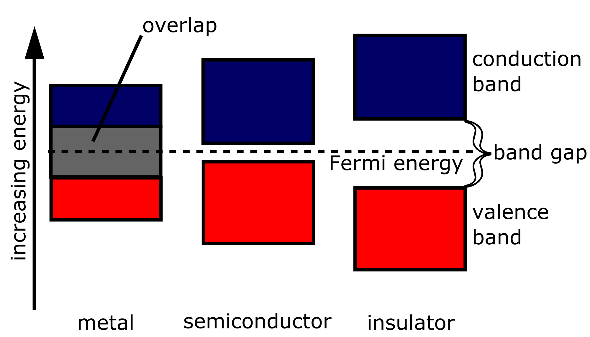
Band gap
As a band gap (English band gap ), and band gap or forbidden zone, the energy gap between the valence band and conduction band of a solid is called. Meanwhile, electrical and optical properties are mainly determined by the size of the band gap. The size of the band gap is usually expressed in electron volts (eV).
- 3.1 Direct bandgap
- 3.2 indirect bandgap
Origin
After the band model of bound states of the electrons are only allowed on certain intervals of the energy scale, the bands. Between the bands can ( but need not) be energetically forbidden areas. Each of these regions represents a gap between the belts, but it is for the physical properties of a solid, only the possible gap between the highest fully occupied with electron band ( valence band VBM ) and the next higher ( conduction band CBM) crucial. Therefore, the band gap is always the one between the valence and conduction band meant.
The appearance of a band gap in some materials can be understood quantum mechanically by the behavior of electrons in the periodic potential of a crystal structure. This model of quasi-free electrons provides the theoretical basis for the band model.
If the valence band overlaps with the conduction band does not occur bandgap. Is the valence band is not completely occupied by electrons, as the upper not -filled region assumes the function of the conduction band, and consequently it has also here no band gap. In these cases, infinitesimal amounts of energy sufficient to excite an electron.
Effects
Electrical conductivity
Only excited electrons in the conduction band can move virtually free through a solid body and contribute to the electrical conductivity. At finite temperatures by thermal excitation always some electrons in the conduction band, but their number varies greatly with the size of the band gap. Based on this reason, the classification according to conductors, semiconductors and insulators is made. The exact boundaries are blurred, however, one can use roughly the following limits as a rule of thumb:
- Leaders have no band gap.
- Semiconductors have a band gap in the range of 0.1 to ≈ 4 eV.
- Dielectrics have a bandgap greater than 4 eV.
Optical Properties
The ability of a solid to light absorption is linked to the condition, take the photon energy by excitation of electrons. Since no electrons can be excited into the forbidden region between the valence and conduction band, the energy of a photon must exceed the energy of the band gap
Otherwise, the photon can not be absorbed.
The energy of a photon at the frequency ( Ny ) of the electromagnetic radiation coupled by the formula
With Planck's quantum of action
If a solid-state band gap, so it is therefore for radiation below a certain frequency / above a certain wavelength transparent (generally, this statement is not entirely correct, since there are also other ways to absorb the photon energy ). Especially for the transmission of visible light ( photon energies around 2 eV ), the following rules can be derived:
Since the absorption of a photon by the excitation of an electron from the valence band into the conduction band is connected, there is a correlation with the electric conductivity. In particular, the electrical resistance of a semiconductor with increasing light intensity, which can be used eg for brightness sensors decreases, see also photo line.
Species
Direct bandgap
The minimum of the conduction band is located in the diagram directly above the maximum of the valence band; it is the wave vector, which is proportional to photons in their vectorial pulse:
With the reduced Planck 's constant
In a direct transition from the valence band to the conduction band of the smallest distance between the bands is directly above the maximum of the valence band. Therefore, the change, the momentum transfer of the photon is neglected because of its small size in comparison.
Examples of applications: light emitting diode
Indirect bandgap
With an indirect band gap, the minimum of the conduction band is shifted from the maximum of the valence band on the axis, i.e. the minimum distance between the belts is displaced. The absorption of a photon is effective only possible with a direct band gap, with an indirect band gap, an additional quasi-momentum () must be involved, with a suitable phonon is created or destroyed. This process a photon is only much less likely because of the low pulse of light, the material has a weaker absorption there.
The best-known semiconductor, silicon, has an indirect band transition.
Temperature dependence
The energy of the band gap decreases with increasing temperature (due to the thermal expansion of the grid ) is first square, then more or less linearly, and starting from a maximum value at. This dependence can be explained phenomenologically inter alia, described by the Varshni formula:
With the Debye temperature
The Varshni parameters can be specified for different semiconductors:


